
Wafer cleaning
Match cleaning to the surface, chemistry and process sequence.

We are here for you
sales[at]exateq.deWe are here for you
+49 9181 4636422Information on engaging topics
Insights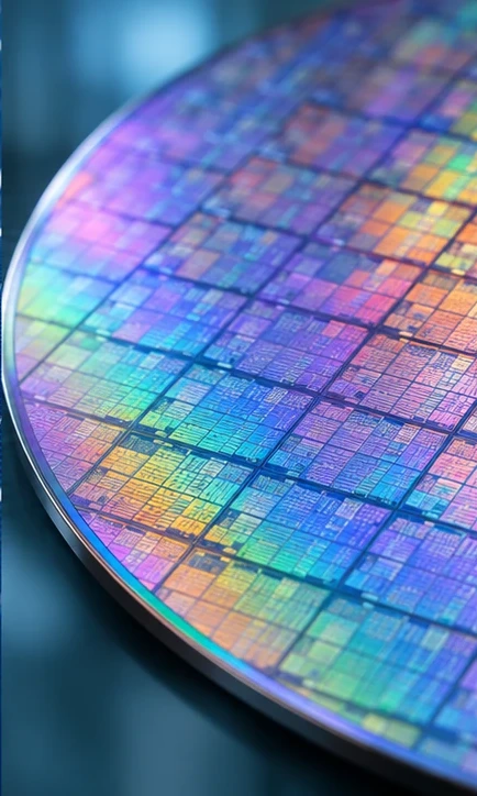
Cleaning wafers, etching layers and developing photoresist.
Match cleaning to the surface, chemistry and process sequence.

Match etching steps to the layer and process objective.

Plan development and rinsing as a sequence.
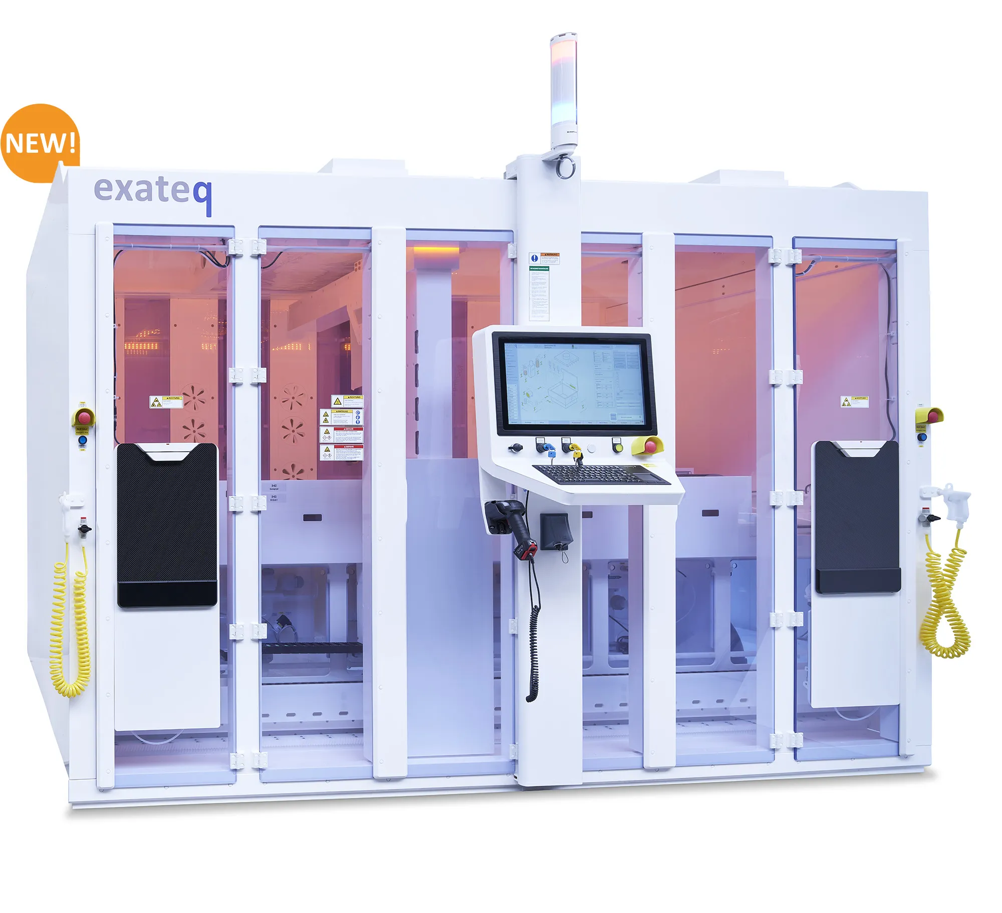
The qSPRINT platform can be configured around the process sequence, substrate and production integration.
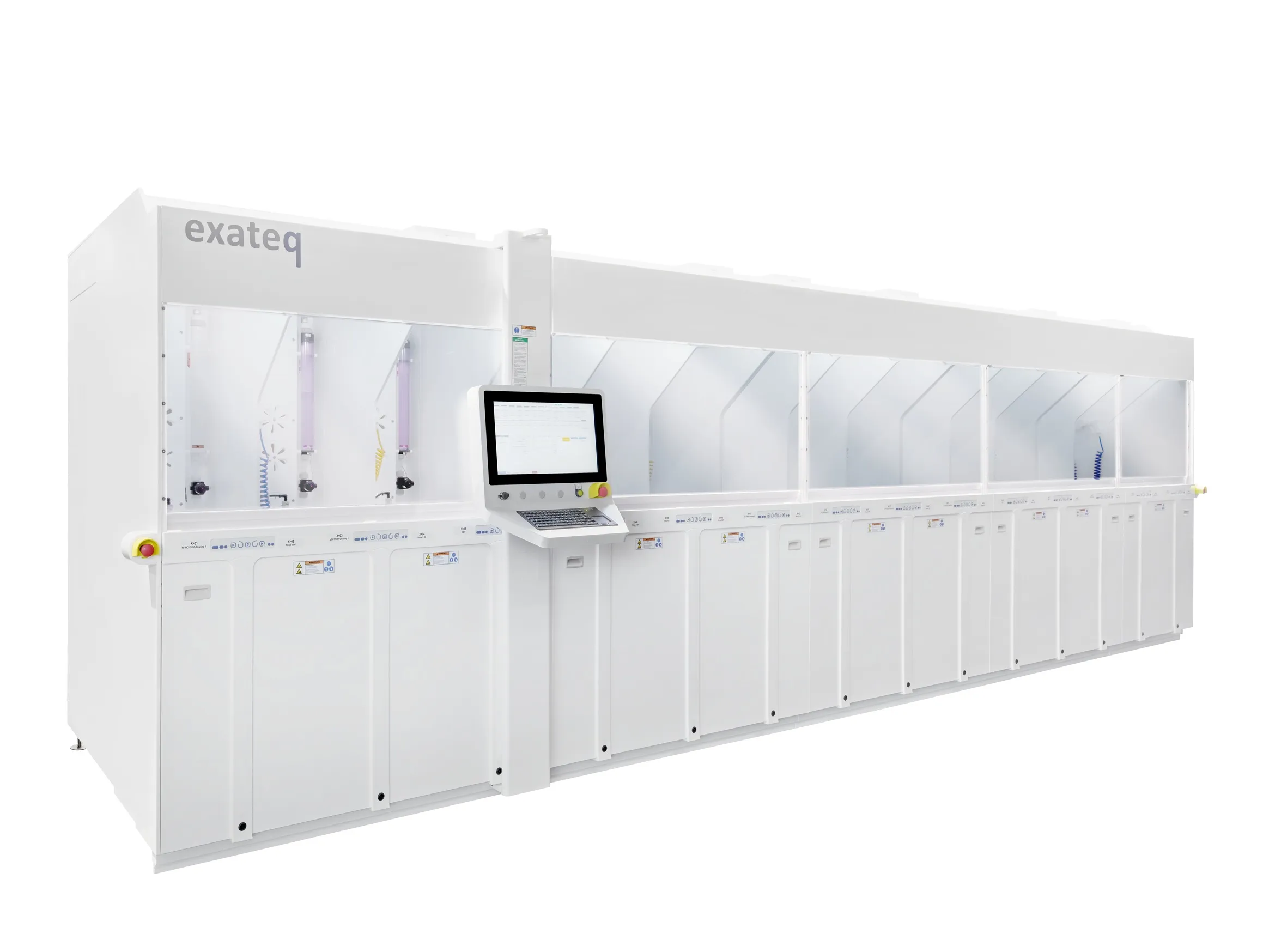
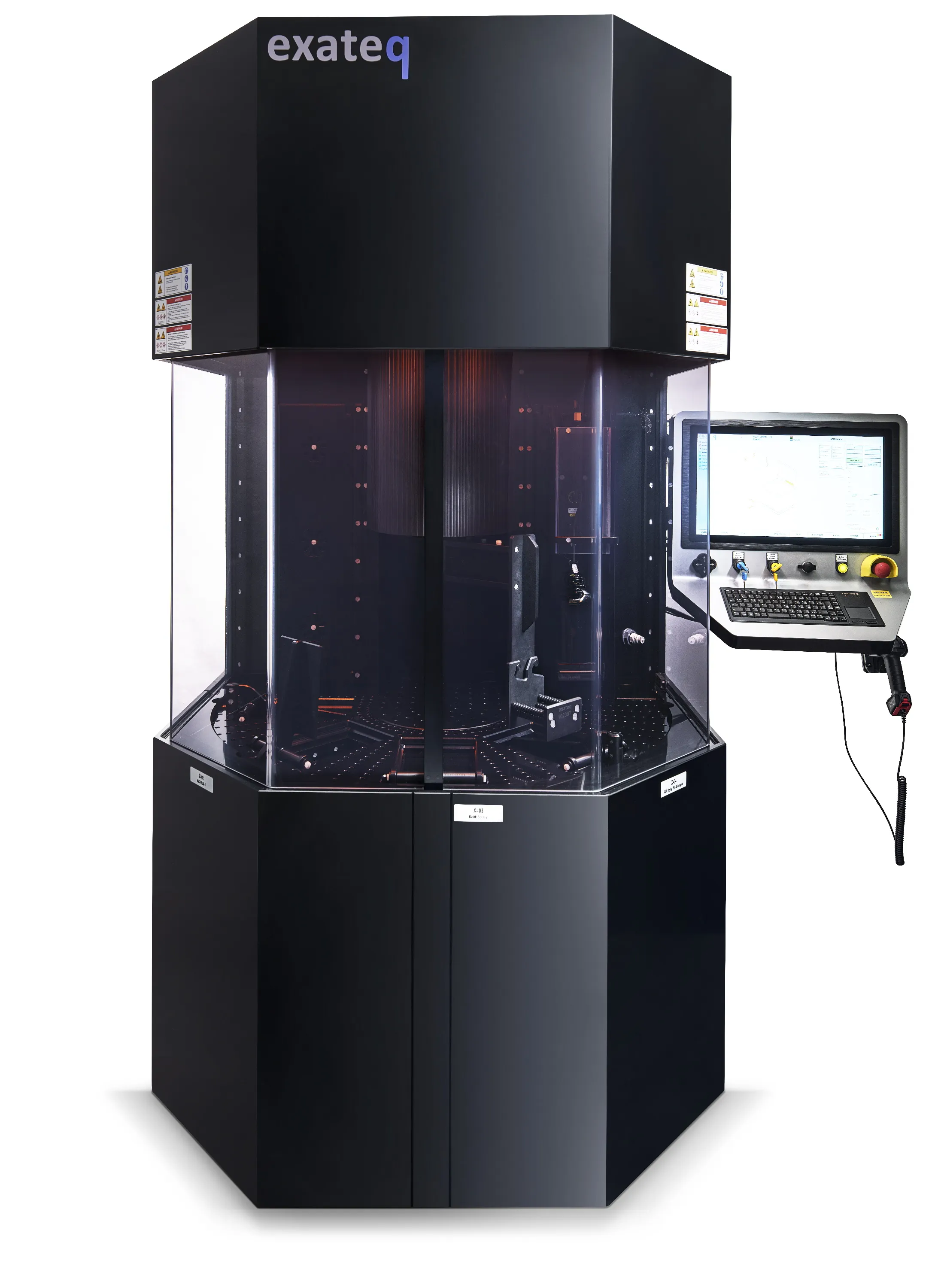
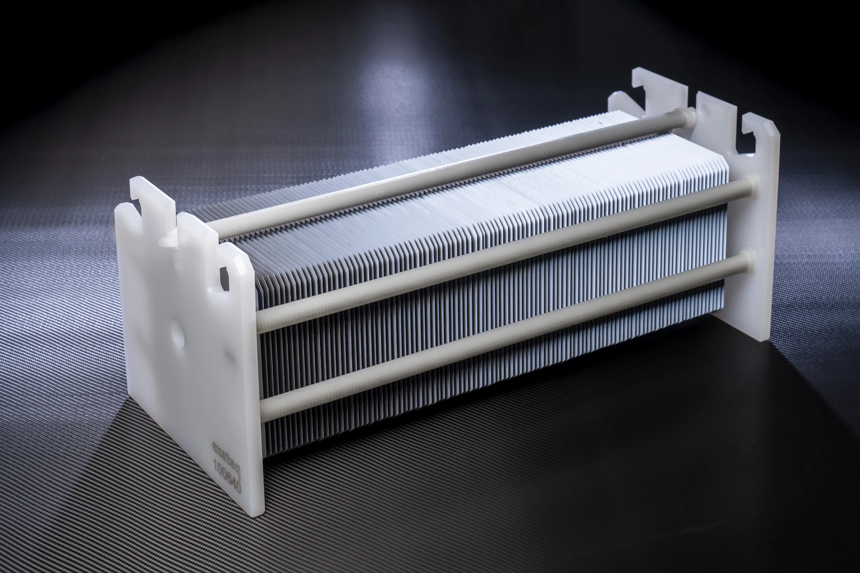
Explore the productWe design and manufacture wet benches for use across a wide range of industries. Although they share many common features, the systems can vary significantly in terms of their structure, size and process requirements, depending on the specific application. A key characteristic of wafers for semiconductor applications is their round shape. This results from the manufacturing process, whereby wafers are sliced from single-crystal ingots. The circular geometry ensures optimal utilisation of the material. Typically, these are rigid disks with a thickness of at least 500 µm and a diameter ranging from 2 inches up to 300 mm. The latter is used in the high-end electronics manufacturing segment, where extreme cleanliness and flawless surface quality are essential. In such production environments, virtually no particle contamination can be tolerated, and the wafer surfaces must exhibit a highly polished, defect-free finish. This requires exceptionally homogeneous process conditions at every stage, along with very high transfer speeds between chemical baths. Although the requirements are less critical for smaller wafer sizes, it is often necessary to process different formats within the same wet process system - while achieving the same high-quality surface finish.
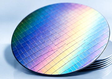 Silicon wafers
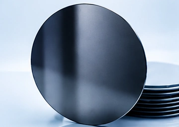 Silicon carbide (SiC)
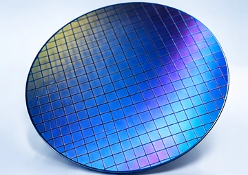 Gallium nitride (GaN)
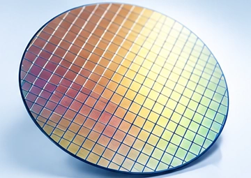 Gallium arsenide (GaAs)